The advancement in technology has brought in many beneficial innovations that help us carry out important tasks such as communication, transportation and even healthcare. Some of the recent breakthroughs include automation, wireless connectivity, remote sensing and monitoring and many more. Electronic devices are getting smaller and more lightweight.
One of the key elements inside an electronic device is the Printed Circuit Board or PCB. The key challenge in the assembly of an electronic device is the design, fabrication and assembly of a PCB that will fit in a small form factor device. To adapt to the demand for miniaturized devices, a new PCB substrate type that is flexible, bendable and versatile was developed. This type of substrate is also known as Flex PCB.
In this article, flex PCB assembly is explained, along with its importance in wearable technology.

What is a Flex PCB?
A flex PCB is a shortened term for a flexible printed circuit board which is a type of PCB with the circuit on a flexible polymer laminate such as polyimide or polyester material. Contrary to rigid PCB, a flex PCB can be bent, twisted and even folded to a particular form or configuration.
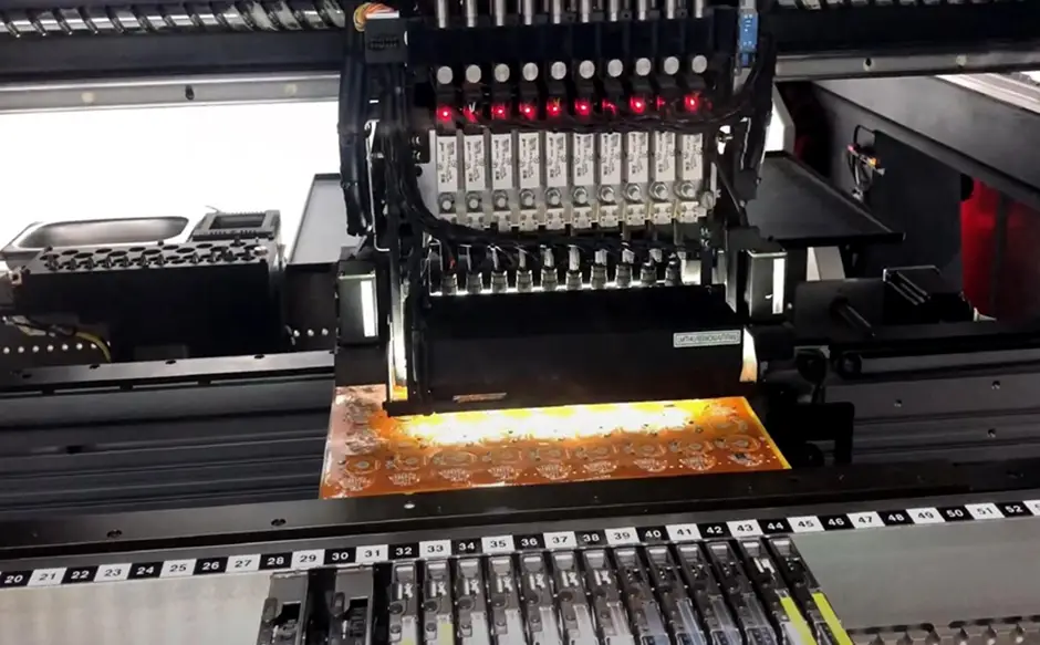
It also follows the same sequence as the assembly of rigid PCB. These processes are also popularly known as Surface Mount Technology or SMT. Since flex PCB is more lightweight, a special fixture is used so that the boards will not be displaced when they pass through the SMT processes.
- Screen Printing. The solder pattern from a stencil is transferred to the bare PCB using screen printing. In the rigorous flex PCB board assembly, solder paste must be uniformly distributed into the opening of the stencils for even placement of components.
- Component Mounting. The components are mounted using a high-speed SMT machine.
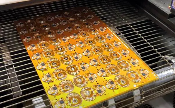
- Reflow. The circuit boards are subjected to a reflow process to achieve a fully cured solder joint.
- Inspection and Testing. The assembled flex PCB is inspected using automated vision systems. Electrical testing is then performed to screen out anomalies in the units.
In several cases, double sided flex PCB assembly is done by first doing the SMT process on the top side and flipping the circuit board to perform SMT on the other side.
What are the Key Components of Flex PCB?
The structure and key components of flex PCB are explained in the following section.
- Substrate. High-temperature grade polymers such as polyimide or polyester are used as substrate materials for flex PCB.
- Conductive Layer. Copper is the most used conductive layer for flex PCB. The conductive layer provides the electrical connection between components.
- Bonding Adhesive. The adhesive is the material used to bond the conductive layers. It can be made of acrylic, epoxy or polyimide prepreg.
- Cover-lay. A cover-lay is added to the flex PCB to shield the circuit from external factors such as temperature and humidity. The cover-lay also provides additional stiffness to the PCB.
What are the Different PCB Types Used in the Flex PCB Assembly?

There are also various types of flex PCBs that are based on the number of conductive layers. The number of layers can impact the overall stiffness of the flex PCB due to the allowable bend radius of the PCB. Here are the common types.
- Single Layer PCB. A single-layer PCB has only one conductive layer, making it the least-cost type of PCB. It is the most used type for flex PCB assembly.
- Double Layer PCB. A double-layer PCB has two conductive layers with an insulating layer sandwiched in between. Plated through holes are drilled through the boards to connect the layers.
- Multi-Layer PCB. Multi-layer PCBs have more than two conductive layers separated by insulating layers. This type of PCB is used for high-density circuits and often consists of vias that are either blind or buried.
What are the Advantages of Flex PCB?
Flex PCB offers several advantages making it a suitable solution for wearables technology.
Like Us on Facebook!
- Flexibility. As the name suggests, flex PCB’s main advantage is its flexibility. This attribute allows flex PCB to conform to various shapes and sizes. Since wearables need to conform to the surface of the body, flex PCBs can be assembled and bent into preferred geometries, unlike rigid PCBs. So flex PCB assembly has a force in the current PCB fabrication market.
- Lightweight. Another benefit of flex PCB is that it is relatively thin and lightweight compared to rigid PCBs. These characteristics are favourable for wearables wherein user comfort is paramount. The overall size and weight of the final product are significantly reduced by using flex PCBs.
- Durability. Flex PCB can perform well under dynamic stresses making it a reliable choice for many wearables applications. The number of times that a flexible substrate can be bent and folded, also referred to as flexing cycles, is being determined to understand the durability of the PCB.
- Ease of Assembly. Due to its flexibility, flex circuits can easily be installed and connected with the rest of the electronic parts. Electronics manufacturing costs are reduced when compared with complex wirings.
- Performance and Functionality. Flex PCBs can provide excellent thermal and consistent electrical performance when in operation. With its ductility, flex circuits can withstand vibrational stresses. Flex PCB can also be integrated with rigid PCB to optimize functionality.
What are the Different Applications of Flexible PCBs in Wearables?

The technology of wearables has a wide range of applications. They are highly useful in medical and consumer electronics. Below are some of its vital applications in wearables.
Subscribe Us on YouTube!
- Health Monitoring Devices. Medical wearables are attached to the skin to monitor vital health information such as blood pressure, sugar and oxygen levels. Flex PCBs broaden medical devices’ capabilities by incorporating sensors for accurate measurements.
- Smart Watches. Smartwatches have also gained popularity due to their vast capabilities such as heart rate monitoring and step count for fitness tracking. These watches have flexible circuits that enable compact and lightweight design.
- Smart Clothing. The world of fashion also keeps up with the technological advancement in electronics. Flex PCBs are being seamlessly integrated into smart clothing to add functionalities like temperature regulation and data transmission.
- Augmented Reality. Augmented reality using smart glasses is also gaining traction in many industries due to its usefulness in engineering and prototyping applications. Flex PCB in A/R systems provides wireless connectivity, motion sensor capabilities and high digital images.
What are the Current Trends and Drivers in Flexible PCBs and Wearable Technology?
PCB assembly services affect the quality of PCB so we need to keep an eye on the current trends of assembly technique revolution. Below are some of the trends that motivate further development of flexible PCBs.
- Internet of Things. The vast proliferation of IoT or the Internet of Things to many significant industries also benefits from flexible PCBs. Sensors, processors and vision systems are seamlessly integrated inside advanced devices due to the versatility of flex-printed circuit boards.
- Energy Supply and Storage. Wearables also require flexible PCBs to support energy storage and supply for prolonged operation. Batteries with flex circuits are well tucked inside wearables that come unnoticed, maintaining sleek appearances.
- Miniaturization. One of the main drivers is the unstoppable direction towards smaller devices. Rigid PCBs have geometric constraints which can be addressed by flex PCBs. Bulky connectors can be replaced by flex circuits in many electronic assemblies.


