
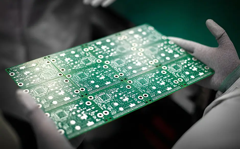
The present-day generation is experiencing major technological advancement in every field. Printed Circuit Boards (PCBs) have played a significant part in this evolution by providing a base for the specifications and enhancing the user experience. The PCBs represent the specific circuit of any application or specification in hardware form. Integrating all the elements of the circuit into the product and PCB form is critical for designers and assembly solution providers. In the evolution of technologies and products, the requirement of multipurpose products having all the required features within a single entity has become a prime concern for all. Due to this the core circuit has become more complex including numerous components. Without affecting the end size of the product, PCBs are now designed with high-density processes. Thus, HDI PCBs came into existence to fulfil this challenge.
What is HDI PCB?
HDI PCB is a circuit board with higher wiring density than traditional PCB. This type of PCB uses advanced manufacturing techniques such as micro holes, blind holes, and buried holes to create smaller and more efficient designs. Although these circuits are highly dense, with the support of technology, this PCB can effectively reduce signal loss and improve signal integrity, making it an ideal choice for compact high-performance devices.
Key Aspects of HDI PCB
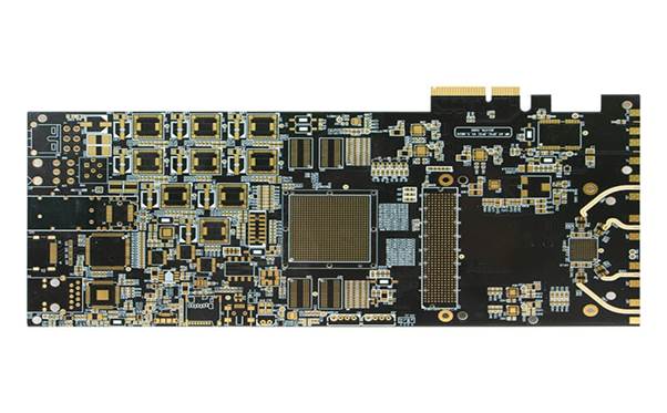
- Multiple Layer Stackup – The length-to-width and height ratio is fixed in all the cases which cannot be altered due to product and end-user restrictions. Earlier PCBs used to have single or both side component arrangements. With the increase in component density and restricted scope for the complete dimensions, the concept of multiple layers came into existence. Each layer contains a part of the circuit. These layers are stacked onto each other with the defined layout and circuit continuity. The final PCB assembly with a multiple-layer stackup forms a complete product.
- Fine Line, Pitches and Drills – The inside parts of the HDI circuit boards such as tracks, traces and component drills are also in very short sizes. This precise calculation is done by keeping the components into consideration. Adequate spacing is also maintained while preparing the PCB layouts for manufacturing. Additional insulation is also provided to avoid cross-connections and shorting issues.
- SMD and Smaller Component Packages – The overall size of the PCB components needs to be smaller and more compact than the regular component version. The core functionality must not be affected while going for the SMD and compact component packages. With the advancement in technology, the PCB components are available in many compact versions according to the application requirements.
- Blind and Buried Vias – To make internal connections among the multiple layers of the PCB, the vias are used in PCB manufacturing. These vias can make continuity between two layers to multiple layers. Based on the nature of the connection, the vias can be blind & buried type. These vias are placed with more accuracy to make exact connections into PCB assembly.
- High-grade Material – The regular material for PCB manufacturing is not suitable for HDI board manufacturing. High-grade material with the capability to handle complex circuit integration, high power handling characteristics, and low loss is developed for HDI circuit board applications. Continued research is also under process to identify and develop more suitable PCB material.
Importance of HDI PCB in Modern Electronics
All the fields and applications require a PCB device with the required features. The product requirements and specifications are becoming more complex with an increase in the feature numbers. The end user is interested only in the external parameters of the product and has little interest in the product and PCB design. Achieving all the required features in a unit becomes more challenging for PCB designers and manufacturers.
- Compact Size and Form Factor – If the PCB is designed by following the circuit layout continuously, then it will result in a large product format. However, the overall dimensions and form factor must be maintained to manufacture a reliable product. HDI PCBs are incorporated with larger circuits to create compact dimensions. Smaller component packages, multilayer arrangement, and the latest circuit design topologies made it quite possible to achieve bigger circuits in small PCB units.
- More Reliable Solution with Enhanced Performance – It may seem that the compact size of the PCB will compromise the product performance. But, in fact, there may be no degraded overall performance of the end product. HDI circuit boards actually have greater reliability and improved performance compared with regular PCB solutions. This is because of adapting newer trends and technology into PCB design and manufacturing.
- Incorporated with the Latest Technology – PCBs have evolved with the continuous development in electronics and technology. The necessity of HDI and a compact version of PCB was later realized due to form factor challenges with modern circuit layouts. Hence the HDI circuit boards are already equipped with the latest technology. All the associated components and processes are also built by applying the modern approach to it.
- Power Efficiency – By theory, the larger circuits consume more power due to an increase in the components and traces. Also, the PCB losses will be higher in similar cases. These kinds of power and efficiency issues have been successfully controlled in the HDI boards. The tiny and compact component packages consume less power compared with the respective conventional PCB components. Also, the minimum length of the traces provides a faster mode of power and data transfer into the PCB.
- Cost-effective Solution – Initially the setup cost is higher even in the case of the HDI board manufacturing and assembly. During the bulk production of the PCB components and final PCB assembly, the overall costs are reduced effectively. The improved version of the component and PCB also has a lower rejection ratio and fault ratio, which in the end improves the overall operational expense.
Conclusion
HDI PCBs have some key aspects that make them unique from the rest of PCB kinds. HDI circuit boards support all the present challenges in PCB design and manufacturing like the integration of numerous components into the required areas, improved performance & overall characteristics. The demand for compact PCBs is always going to increase. In the coming time, more efficient and improved PCB manufacturing practices will come onto the scene with better results. So printed circuit board manufacturers should keep pace with the incoming technologies and apply them to the product.